


-
1
-
2
-
3
-
4
-
5
-
6
-
7
-
8
-
9
-
10
-
11
-
12
-
13
-
14
-
15
-
16
-
17
-
18
-
19
-
20
-
21
-
22
-
23
-
24
-
25
-
26
-
27
-
28
-
29
-
30
-
31
-
32
-
33
-
34
-
35
-
36
-
37
-
38
-
39
-
40
-
41
-
42
-
43
-
44
-
45
-
46
-
47
-
48
-
49
-
50
-
51
-
52
-
53
-
54
-
55
해당 자료는 10페이지 까지만 미리보기를 제공합니다.
10페이지 이후부터 다운로드 후 확인할 수 있습니다.
10페이지 이후부터 다운로드 후 확인할 수 있습니다.


목차
프로젝트 전체 진행 계획 및 구성
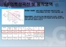
업무분담
기초 이론
1단 및 2단 증폭기
최종설계
업무분담
기초 이론
1단 및 2단 증폭기
최종설계
본문내용
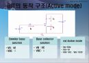
Design and simuation of maximum amplifier circuit
Limitations
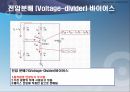
1) Must use transistor
(use of cascaded transistor is recommended)
2) Gain : over 50 dB (voltage gain when 8 ohm load is connected)
3) Bandwidth : 200Hz ~ 30,000 Hz (-3dB BW)
To do list
1) Term project
- Introduction: application and significance of the chosen amplifier
circuit
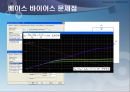
- Simulation: PSPICE input and result files (must show gain and
bandwidth)
- Analysis and Discussion of the PSPICE circuit simulations
Conclusions
Limitations
1) Must use transistor
(use of cascaded transistor is recommended)
2) Gain : over 50 dB (voltage gain when 8 ohm load is connected)
3) Bandwidth : 200Hz ~ 30,000 Hz (-3dB BW)
To do list
1) Term project
- Introduction: application and significance of the chosen amplifier
circuit
- Simulation: PSPICE input and result files (must show gain and
bandwidth)
- Analysis and Discussion of the PSPICE circuit simulations
Conclusions
- 가격3,000원
- 페이지수55페이지
- 등록일2021.03.19
- 저작시기2021.3
- 파일형식파워포인트(ppt)
- 자료번호#1146658

본 자료는 최근 2주간 다운받은 회원이 없습니다.


소개글