


-
1
-
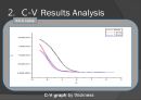
2
-
3
-
4
-
5
-
6
-
7
-
8
-
9
-
10
-
11
-
12
-
13
-
14
-
15
-
16
-
17
-
18
-
19
-
20
-
21
-
22
-
23
-
24
해당 자료는 8페이지 까지만 미리보기를 제공합니다.
8페이지 이후부터 다운로드 후 확인할 수 있습니다.
8페이지 이후부터 다운로드 후 확인할 수 있습니다.


목차
1. 실험목적
2. 실험과정
3. 결과분석
4. 결론
5. 참고문헌
2. 실험과정
3. 결과분석
4. 결론
5. 참고문헌
본문내용
Purpose of the Experiment
Understanding the principle and characteristics of the MOS Capacitor
C-V, I-V analysis in accordance with the thickness of the Al2O3 insulator
Insulator thickness (6nm, 12nm, 18nm)
Experimental Background
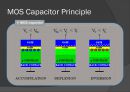
MOS Capacitor
MOS Capacitor structure
MOS Capacitor principle
<중 략>
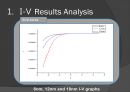
1. I-V Results Analysis
Negative Voltage applied
Break down tendency
Current increase section
current at thickness 12nm > currents at thickness 6nm and 18nm
Guess cause of the error
(1) Breakdown voltage
(2) Skin effect : Depending humidity or the shape of the surface, there is a large variation
(3) No annealing process
(4) It is dependent on the surronding conditions such as humidity and surface internal temperature
Understanding the principle and characteristics of the MOS Capacitor
C-V, I-V analysis in accordance with the thickness of the Al2O3 insulator
Insulator thickness (6nm, 12nm, 18nm)
Experimental Background
MOS Capacitor
MOS Capacitor structure
MOS Capacitor principle
<중 략>
1. I-V Results Analysis
Negative Voltage applied
Break down tendency
Current increase section
current at thickness 12nm > currents at thickness 6nm and 18nm
Guess cause of the error
(1) Breakdown voltage
(2) Skin effect : Depending humidity or the shape of the surface, there is a large variation
(3) No annealing process
(4) It is dependent on the surronding conditions such as humidity and surface internal temperature
키워드
추천자료
 Al2O3의 EDTA킬레이트 역적정법에 의한 정량
 Fe2O3와 TiO2의 특성 및 응용분야
- Li2O-Al2O3-SiO2 (LAS)계와 MgO-Al2O3-SiO2 (MAS)계
- Al2O3와 BaTio3의 제조
- Oxidation 공정과 Evaporation 을 통해 제작한 nMOS capacitor 소자의 전기적 특성
 Slip casting을 이용한 고밀도 ZnO-Al2O3 제조
- [전자재료실험] MOS Capacitor
- MOS Capacitor(커패시터)의 제작 방법과 특성와 C-V등을 측정 - MOS Capacitor의 제작 방법과...
- 산화층 두께에 따른 MOS Capacitor의 C-V 및 I-V 그래프 변화 분석
- 가격3,000원
- 페이지수24페이지
- 등록일2014.01.07
- 저작시기2013.5
- 파일형식기타(pptx)
- 자료번호#901286

본 자료는 최근 2주간 다운받은 회원이 없습니다.


소개글