


-
1
-
2
-
3
-
4
-
5
-
6
-
7
-
8
-
9
-
10
-
11
-
12
-
13
-
14
-
15
-
16
-
17
-
18
-
19
-
20
-
21
-
22
-
23
-
24
-
25
-
26
-
27
-
28
-
29
-
30
-
31
-
32
-
33
-
34
-
35
-
36
-
37
-
38
-
39
-
40
-
41
-
42
-
43
-
44
-
45
-
46
-
47
-
48
-
49
해당 자료는 10페이지 까지만 미리보기를 제공합니다.
10페이지 이후부터 다운로드 후 확인할 수 있습니다.
10페이지 이후부터 다운로드 후 확인할 수 있습니다.


목차
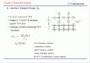
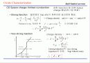
Ⅰ. C-V Introduction
Ⅱ. I-V measurement
1. Introduction
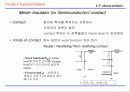
2. Metal-Insulator contacts
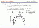
3. Image-force effect
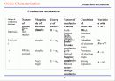
4. Conduction mechanism
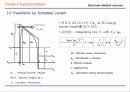
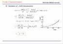
(1) Electrode-limited current
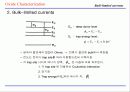
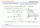
(2) Bulk-limited current
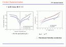
5. 실제 Data 해석
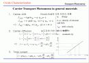
Ⅱ. I-V measurement
1. Introduction
2. Metal-Insulator contacts
3. Image-force effect
4. Conduction mechanism
(1) Electrode-limited current
(2) Bulk-limited current
5. 실제 Data 해석
본문내용
C-V Introduction
Ideal MOS Capacitor
구조
특징
Gate는 두꺼워서 언제나 등전위 영역
Oxide는 perfect Insulator
Oxide 내에서나 S/C-Oxide 계면에서 charge center 없다.
S/C는 uniform doping
S/C는 충분히 두꺼워서 gate potential을 가하든지 아니든지
bulk는 field-free 영역이다.
S/C와 metal 사이에는 ohmic contact(non-rectifying contact)
MOS-C의 변수들은 x에 의해서 변하는 1차원적인 구조
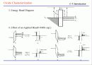
3. Energy Band Diagram
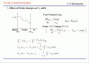
4. Effect of an Applied Bias(P-MOS cap.)
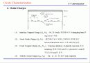
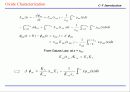
5. Charge Distribution (dc bias + ac bias )
Accumulation
Depletion
Inversion (low frequency)
Inversion (high frequency)
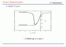
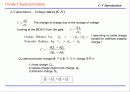
6. Ideal C-V curve
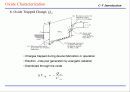
7. Deep Depletion : DC bias와 AC bias 가 모두 빨리 변하는 경우
Inversion layer를 형성하지 못하고 depletion layer가 커짐.
Minority carrier generation 속도가 dc Gate bias 변화 속도를 따라가지 못함
→
minority carrier에 의해 상쇄되는 전하의 수가 감소
→
상쇄되지 않은 majority carrier에 의해 depletion layer 두께가 maximum 보다 커짐.
Minority carrier가 하나도 없을 때를 total deep depletion
Ideal MOS Capacitor
구조
특징
Gate는 두꺼워서 언제나 등전위 영역
Oxide는 perfect Insulator
Oxide 내에서나 S/C-Oxide 계면에서 charge center 없다.
S/C는 uniform doping
S/C는 충분히 두꺼워서 gate potential을 가하든지 아니든지
bulk는 field-free 영역이다.
S/C와 metal 사이에는 ohmic contact(non-rectifying contact)
MOS-C의 변수들은 x에 의해서 변하는 1차원적인 구조
3. Energy Band Diagram
4. Effect of an Applied Bias(P-MOS cap.)
5. Charge Distribution (dc bias + ac bias )
Accumulation
Depletion
Inversion (low frequency)
Inversion (high frequency)
6. Ideal C-V curve
7. Deep Depletion : DC bias와 AC bias 가 모두 빨리 변하는 경우
Inversion layer를 형성하지 못하고 depletion layer가 커짐.
Minority carrier generation 속도가 dc Gate bias 변화 속도를 따라가지 못함
→
minority carrier에 의해 상쇄되는 전하의 수가 감소
→
상쇄되지 않은 majority carrier에 의해 depletion layer 두께가 maximum 보다 커짐.
Minority carrier가 하나도 없을 때를 total deep depletion
키워드
추천자료
- 가격3,000원
- 페이지수49페이지
- 등록일2005.04.21
- 저작시기2005.04
- 파일형식파워포인트(ppt)
- 자료번호#293788

본 자료는 최근 2주간 다운받은 회원이 없습니다.


소개글