


-
1
-
2
-
3
-
4
-
5
-
6
-
7
-
8
-
9
-
10
-
11
-
12
-
13
-
14
-
15
-
16
-
17
-
18
-
19
-
20
-
21
-
22
-
23
-
24
-
25
-
26
-
27
-
28
-
29
-
30
-
31
-
32
-
33
-
34
-
35
-
36
-
37
-
38
-
39
-
40
-
41
-
42
-
43
-
44
-
45
-
46
-
47
-
48
-
49
-
50
-
51
-
52
-
53
-
54
-
55
-
56
-
57
-
58
해당 자료는 10페이지 까지만 미리보기를 제공합니다.
10페이지 이후부터 다운로드 후 확인할 수 있습니다.
10페이지 이후부터 다운로드 후 확인할 수 있습니다.


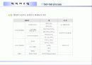
목차
** Evaporation **
1. 서 론
2. Deposition Mechanism
3. Thickness measurement
4. Thin film growth process
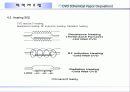
5. Heating source
6. Deposition of materials
7. Deposition 의 종류
8. Properties of evaporated films
** Sputtering **
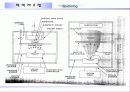
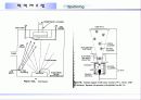
1. 서론
2. Gas Discharge의 원리
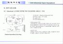
** CVD (Chemical Vapor Deposition) **
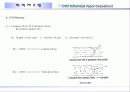
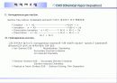
1. CVD (Chemical Vapor Deposition)
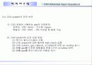
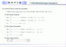
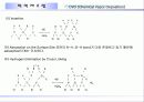
3. CVD의 종류
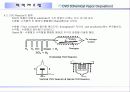
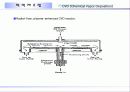
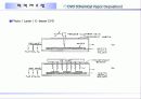
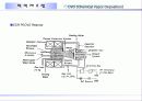
4. CVD Reactor
5. CVD Kinetics
6. LPCVD
7. Si, SiO2, Si3N4 박막형성 공정
8. 저온 CVD 공정
9. PECVD
** Sol-Gel process **
1. Sol-Gel 법의 발전
2. Sol-Gel 법이란
3. Sol-Gel 법의 원료
4. 금속 알콕사이드
5. Sol-gel 반응
6. Si(OR)4의 가수분해 및 중축합 반응
7. Sol-gel 법으로 제작한 코팅막
8. 졸-겔법의 장점 및 단점
9. 졸-겔 과정의 연구에 응용되는 특성분석 방법
10. 세라믹스 박막으로의 응용
1. 서 론
2. Deposition Mechanism
3. Thickness measurement
4. Thin film growth process
5. Heating source
6. Deposition of materials
7. Deposition 의 종류
8. Properties of evaporated films
** Sputtering **
1. 서론
2. Gas Discharge의 원리
** CVD (Chemical Vapor Deposition) **
1. CVD (Chemical Vapor Deposition)
3. CVD의 종류
4. CVD Reactor
5. CVD Kinetics
6. LPCVD
7. Si, SiO2, Si3N4 박막형성 공정
8. 저온 CVD 공정
9. PECVD
** Sol-Gel process **
1. Sol-Gel 법의 발전
2. Sol-Gel 법이란
3. Sol-Gel 법의 원료
4. 금속 알콕사이드
5. Sol-gel 반응
6. Si(OR)4의 가수분해 및 중축합 반응
7. Sol-gel 법으로 제작한 코팅막
8. 졸-겔법의 장점 및 단점
9. 졸-겔 과정의 연구에 응용되는 특성분석 방법
10. 세라믹스 박막으로의 응용
본문내용
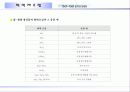
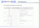
1. 서 론
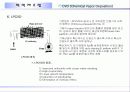
- 1857년 Faraday 개발
- 진공중에서 물질을 가열하여 증발
- 장점 1) 비교적 간단하다( 구성, 물질등)
2) 물성연구에 적합( 핵생성 및 성장, 박막형성의 형태등)
- 단점 1) 접착이 약함
2) Low quality thin film
3) Tm 이 높은 물질 즉 Pt , Ta, Ti, W 등의 증착이 어렵다.
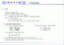
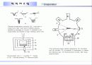
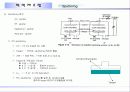
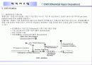
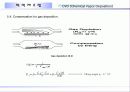
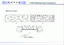
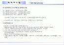
2. Deposition Mechanism
2.1. Hertz -Knudsen Equation
2.2 Mean Free Path ? 평균자유행로
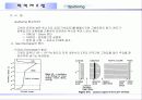
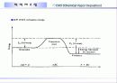
2.3 Variation in deposition rate
to ; thickness at the coated surface directly above or below the source
tx ; thickness of deposition at some distance ,x from the center of the coated surface
h ; distance between source and substrate
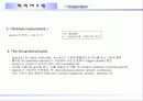
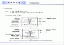
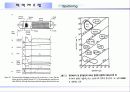
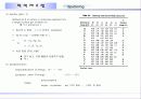
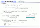
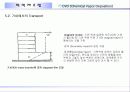
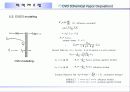
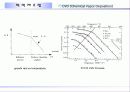
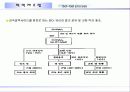
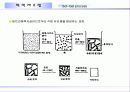
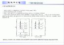
3. Thickness measurement, t
source 의 무게 = 4 π r2 * t
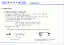
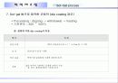
4. Thin film growth process
- Species ( Ex:
- 1857년 Faraday 개발
- 진공중에서 물질을 가열하여 증발
- 장점 1) 비교적 간단하다( 구성, 물질등)
2) 물성연구에 적합( 핵생성 및 성장, 박막형성의 형태등)
- 단점 1) 접착이 약함
2) Low quality thin film
3) Tm 이 높은 물질 즉 Pt , Ta, Ti, W 등의 증착이 어렵다.
2. Deposition Mechanism
2.1. Hertz -Knudsen Equation
2.2 Mean Free Path ? 평균자유행로
2.3 Variation in deposition rate
to ; thickness at the coated surface directly above or below the source
tx ; thickness of deposition at some distance ,x from the center of the coated surface
h ; distance between source and substrate
3. Thickness measurement, t
source 의 무게 = 4 π r2 * t
4. Thin film growth process
- Species ( Ex:
추천자료
 멤브레인을 이용한 고도정수처리 기술 막분리
- 진공증착법을 이용한 박막제작
- PL법 도입과 소송사례를 통한 기업의 대응방안
- [고분자][고분자 제조법][고분자 화합물][고분자 화합물 종류][고분자 복합체][고분자와 플라...
- 폐합성고분자 발생 및 처리현황
- [특허][기업활동][특허 이용관계][특허 선행기술조사][특허 경쟁력 제고 방안]특허의 조건, ...
- [거래, 전자상거래, 할부거래, 차익거래, 내부자거래, 선물거래, REPO거래(환매조건부채권매...
- [벤처창업][벤처][창업][사업화][조직구성][자금지원]벤처창업의 사업화, 벤처창업의 성공조...
- [벤처창업][벤처][창업][자금지원][시장조사]벤처창업의 의미, 벤처창업의 절차, 벤처창업의 ...
- [위험][위험사회][위험범죄][위험방지][위험수위][위험전가][위험부담][위험요인][위험성][위...
- [경영관리][경영][경영관리 정의][경영관리 역사][경영관리 의의][합리성]경영관리의 정의, ...
- [제조업][제조기업][기업]제조업(제조기업)의 서비스화, 제조업(제조기업)의 공동화, 제조업(...
- [공학설계] 신소재프로세스 설계 예시 - 사다리
- [서비스기업에서의 6시그마기법 활용]서비스기업에서의 프로젝트수행절차 및 6시그마 수행기법
- 가격3,000원
- 페이지수58페이지
- 등록일2006.03.20
- 저작시기2006.03
- 파일형식파워포인트(ppt)
- 자료번호#340471

본 자료는 최근 2주간 다운받은 회원이 없습니다.