


-
1
-
2
-
3
-
4
-
5
-
6
-
7
-
8
-
9
-
10
-
11
-
12
-
13
-
14
-
15
-
16
-
17
-
18
-
19
-
20
해당 자료는 7페이지 까지만 미리보기를 제공합니다.
7페이지 이후부터 다운로드 후 확인할 수 있습니다.
7페이지 이후부터 다운로드 후 확인할 수 있습니다.


목차
1. Single crystal bulk
1.1 Theory
1.2 Method of growing single crystal 'KDP'
-\"Aqueous solution method\"
1.3 Result
1.4 Conclusion
2. Single crystal thin film
2.1 Theory
2.2 Method of growing single crystal 'ZnO Film'
-\"Sputtering\"
2.3 Result
2.4 Conclusion
3. Single crystal nanowire
3.1 Theory
3.2 Method of growing single crystal nanowire of ZnO -\" Wet-Chemistry\"
3.3 Result
3.4 Conclusion
4. Reference
본문내용
because of many limitation.
(3)Application of ZnO nanowire
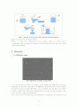
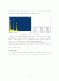
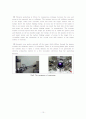
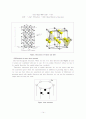
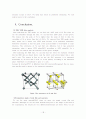
① We can see the ZnO nanowire sturcture that space of Zn atom and O atom is not regular but lean to the up direction. In other words, it has a little bit polarity. By the time it get a pressure, this space is more and more lean to the up direction and has more polarity. So, ZnO make a electricity about 60mA. Therefore, we can apply to a piezoelectric device.
② ZnO nano wire application possibility is confirmed in various field application possibility. Especially, ZnO has wide band gap and higher Exciton combination energy. So in short wavelength field, application is researched heavily as a light electricity device. ZnO application of nano wires is that FETdevice, SETdevice, SAWdevice, Ultraviolet radiation device, Sun electric cell, sensor, Optical fiber, UVsensor, a light switch, a spin device, etc.
Fig20. Application of nanowire
Reference
Theory of Sputtering. I. Sputtering Yield of Amorphous and Polycrystalline Targets - P Sigmund - Physical Review, 1969 - APS
Electrical characterization of vapor-phase-grown single-crystal ZnO - Appl. Phys. Lett. 80, 1340 (2002); doi:10.1063/1.1452781
Single-Crystal Nanorings Formed by Epitaxial Self-Coiling of Polar Nanobelts
Xiang Yang Kong, Yong Ding, Rusen Yang, Zhong Lin Wang*
Growth of ZnO single crystal thin films on c-plane (0001) sapphire by plasma enhanced molecular beam epitaxy- CHEN Y. BAGNALL D. M. ZHU Z. SEKIUCHI T. PARK K.-T. HIRAGA K. YAO T. KOYAMA S. SHEN M. Y. GOTO T.
Excitonic structure and absorption coefficient measurements of ZnO single crystal epitaxial films deposited by pulsed laser deposition - J. Appl. Phys. 85, 7884 (1999); doi:10.1063/1.370601
Heterostructures of ZnOZn coaxial nanocables and ZnO nanotubes - Appl. Phys. Lett. 81, 1312 (2002); doi:10.1063/1.1499512
Initial preferred growth in zinc oxide thin films on Si and amorphous substrates by a pulsed laser deposition - Jae HyoungChoi, Hitoshi Tabata*, Tomoji Kawai
나노와이어의 성장, 한국에너지기술원, 유주현
X-ray single crystal structure analysis 서일환, 1936-. 북스힐, 2001.
Bulk crystal growth of materials / Capper, Peter. John Wiley & Sons , 2005.
Nanotubes and Nanowires . Royal Society of Chemistry , 2005.
Nanowires and nanobelts : materials, properties, and devices /
Wang, Zhong Lin. Kluwer Academic Publishers , 2003.
The Properties Characterization of ZnO Thin Film Grown by Sputtering /S. M. Jung
ZnO film deposition on Al film and effects of deposition temperature on ZnO film growth characteristics / Yoon, Giwan ,
Growth of bulk single crystals under by liquid phase / Sheibani, H
The nano-micro interface: bridging the micro and nano worlds / Fecht, Hans-Jorg. Wiley-VCH , 2004.
Elements of x-ray diffraction / B. D. Cullity.
Crystal Bank(Web page) - KOSEF, 부산대학교
http://blog.naver.com/rhpys?Redirect=Log&logNo=50044333334
http://tpal.skku.ac.kr/equip_cfubm.htm (TPAL박막 공및응용연구실)
psel.snu.ac.kr/psel/files/lecture/sputter
http://thinfilm.snu.ac.kr/flowable.htm
(3)Application of ZnO nanowire
① We can see the ZnO nanowire sturcture that space of Zn atom and O atom is not regular but lean to the up direction. In other words, it has a little bit polarity. By the time it get a pressure, this space is more and more lean to the up direction and has more polarity. So, ZnO make a electricity about 60mA. Therefore, we can apply to a piezoelectric device.
② ZnO nano wire application possibility is confirmed in various field application possibility. Especially, ZnO has wide band gap and higher Exciton combination energy. So in short wavelength field, application is researched heavily as a light electricity device. ZnO application of nano wires is that FETdevice, SETdevice, SAWdevice, Ultraviolet radiation device, Sun electric cell, sensor, Optical fiber, UVsensor, a light switch, a spin device, etc.
Fig20. Application of nanowire
Reference
Theory of Sputtering. I. Sputtering Yield of Amorphous and Polycrystalline Targets - P Sigmund - Physical Review, 1969 - APS
Electrical characterization of vapor-phase-grown single-crystal ZnO - Appl. Phys. Lett. 80, 1340 (2002); doi:10.1063/1.1452781
Single-Crystal Nanorings Formed by Epitaxial Self-Coiling of Polar Nanobelts
Xiang Yang Kong, Yong Ding, Rusen Yang, Zhong Lin Wang*
Growth of ZnO single crystal thin films on c-plane (0001) sapphire by plasma enhanced molecular beam epitaxy- CHEN Y. BAGNALL D. M. ZHU Z. SEKIUCHI T. PARK K.-T. HIRAGA K. YAO T. KOYAMA S. SHEN M. Y. GOTO T.
Excitonic structure and absorption coefficient measurements of ZnO single crystal epitaxial films deposited by pulsed laser deposition - J. Appl. Phys. 85, 7884 (1999); doi:10.1063/1.370601
Heterostructures of ZnOZn coaxial nanocables and ZnO nanotubes - Appl. Phys. Lett. 81, 1312 (2002); doi:10.1063/1.1499512
Initial preferred growth in zinc oxide thin films on Si and amorphous substrates by a pulsed laser deposition - Jae HyoungChoi, Hitoshi Tabata*, Tomoji Kawai
나노와이어의 성장, 한국에너지기술원, 유주현
X-ray single crystal structure analysis 서일환, 1936-. 북스힐, 2001.
Bulk crystal growth of materials / Capper, Peter. John Wiley & Sons , 2005.
Nanotubes and Nanowires . Royal Society of Chemistry , 2005.
Nanowires and nanobelts : materials, properties, and devices /
Wang, Zhong Lin. Kluwer Academic Publishers , 2003.
The Properties Characterization of ZnO Thin Film Grown by Sputtering /S. M. Jung
ZnO film deposition on Al film and effects of deposition temperature on ZnO film growth characteristics / Yoon, Giwan ,
Growth of bulk single crystals under by liquid phase / Sheibani, H
The nano-micro interface: bridging the micro and nano worlds / Fecht, Hans-Jorg. Wiley-VCH , 2004.
Elements of x-ray diffraction / B. D. Cullity.
Crystal Bank(Web page) - KOSEF, 부산대학교
http://blog.naver.com/rhpys?Redirect=Log&logNo=50044333334
http://tpal.skku.ac.kr/equip_cfubm.htm (TPAL박막 공및응용연구실)
psel.snu.ac.kr/psel/files/lecture/sputter
http://thinfilm.snu.ac.kr/flowable.htm
추천자료
 동북공정 분석과 올바른 대응
- P/M법과 Casting의 공정 데이터 분석
- [미디어선거보도][민주주의][미디어선거][선거보도]미디어선거보도에 있어 민주주의, 바람직...
- [소프트웨어][소프트웨어개발][소프트웨어개발모형][프로그램]소프트웨어의 특성과 소프트웨...
- [제조법][제조방법][제조][제조공정][제조과정]한지의 제조법, 숯의 제조법, 삼베와 모시의 ...
- [MOS][CMOS][MOS의 원리][MOS의 제조공정][CMOS의 원리][CMOS의 인터페이스][CMOS 논리계열][...
- 학교교육(공교육)의 의의와 불공정성, 학교교육(공교육)의 질, 학교교육(공교육)과 교육복지,...
- [MP3][MP3 특징][MP3 공정이용][MP3 다운로드][MP3 응용분야][MP3 문제점][MP3 관련 제언]MP3...
 결합서비스의 사례와 불공정경쟁 이슈 분석
 - 중국의 이어도 공정의 실체분석과 한국의 바람직한 대응방안
- 라면의 역사와 제조공정 및 문제점 분석조사
- [법리, 공용침해, 부정경쟁]공용침해의 법리, 부정경쟁의 법리, 영업비밀보호의 법리, 영업양...
- [미국, 산업기술]미국의 산업기술, 미국의 정보기술(IT), 과학기술, 미국의 신공정기술, 웹기...
- 인사고과제도(근무평정제도, 업적평가제도)의 특성, 의의, 인사고과제도(근무평정제도, 업적...
- 가격1,500원
- 페이지수20페이지
- 등록일2010.01.11
- 저작시기2009.11
- 파일형식한글(hwp)
- 자료번호#572826

본 자료는 최근 2주간 다운받은 회원이 없습니다.


소개글